
The laser light source and line scan camera need to be placed on the upper and lower sides of the object to be measured.
The laser uses its good directionality to penetrate the silicon wafer and form an image on the camera end. Compared with traditional LEDs, it has the advantages of longer wavelength, stronger penetration, high brightness, high uniformity and sharp edge imaging.
The product is compact and can meet more application scenarios.
Parameter Table
| Specification | Parameter |
|---|---|
| Can be used in process section | ☑Raw silicon loading ☑After texturing ☑After back film ☑After positive film ☑Silk screen loading |
| Available for silicon wafer size | ☑182mm ☑210mm ☑230mm |
| External trigger function | ☐5V ☑12V ☐None |
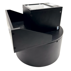
| Product form | ☐Convex ☑L-shaped ☐Other |
| Input voltage | DC 12V |
| Ambient temperature | +10℃~+35℃ |
| Store at temperature | -20°C~+60°C |
© Copyright 2026 Earth Tekniks Pvt Ltd. All Rights Reserved.
Reviews