
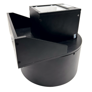
Description
Product features
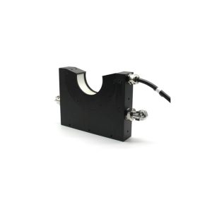
The laser light source and the linear scan camera need to be placed on both sides of the subject.
The laser uses its good directionality to penetrate the silicon wafer and image it on the camera end. Longer wavelength, high brightness, high uniformity and sharp edge imaging than conventional LEDs
Product compact size, can meet more application scenarios
Application areas
Detection of cracks and angle defects in the edge of raw silicon, velvet and etching
Parameters
| Specifications | Parameters |
|---|---|
| Can be used for process segments | ☑ Proto-silicon material ☑ after velvet ☑ back film ☑ front film ☑ façade ☑ filament |
| Available in silicon wafer size | ☑182mm ☑210mm ☑230mm |
| External trigger function | ☐5V ☑12V ☐ None |
| Product form | ☐ convex ☑L shape ☐ Other |
| Input voltage | DC 12V |
| Ambient temperature | +10°CC ~ +35 °C |
| The temperature. | -20°C to +60 °C |


Reviews